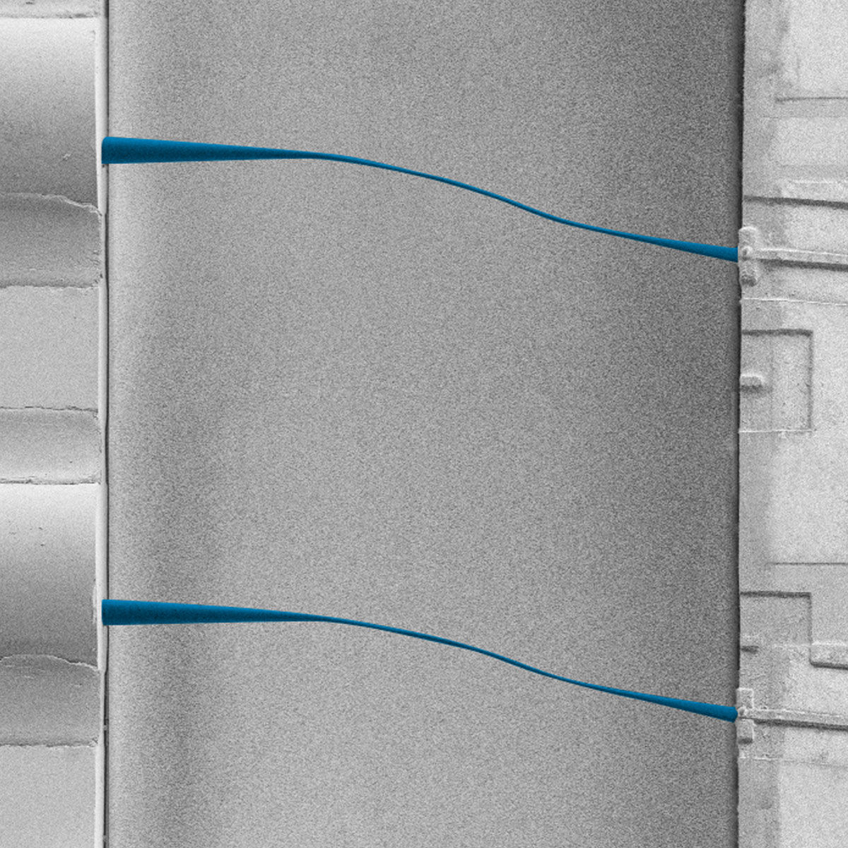
Photonic Wire Bonds
- Adaptable for any design due to software defined additive fabrication
- Compensates vertical and lateral alignment offsets by up to ± 20 µm.
- Flexibility to support standard and non-standard waveguide pitch
Photonic Wire Bonds – the process
Step 1: Assembly build up with passive component alignment and relaxed tolerances ± 20µm
Step 2: Drop dispense photoresist and passive detection of waveguide interfaces
Step 3: Automatic nanofabrication of Photonic Wire Bonds
Step 4: Post development steps and cleaning of the assembly
Step 5: Encapsulation of the Photonic Wire Bonds