Solder paste perfection at jet speed
How jet printing is gaining momentum and versatilitySince its introduction over a decade ago, solder paste jet printing has continued to improve the quality and versatility of electronics manufacturers worldwide. This is especially true in the world of high-mix electronics, where the high accuracy and high flexibility of software-driven assembly processes are crucial to competitiveness. Now, with faster jetting speeds, a wider range of compatible solder pastes and tightly integrated solder paste inspection (SPI) capabilities, jet printing has matured into a powerful platform for increased production efficiency and improved first-pass yield.

The next generation of flexibility
Every day, manufacturers who have adopted jet printing as a replacement for stencil printing confirm their operational, financial and commercial gains. By eliminating lead times and costs associated with sourcing and managing stencils throughout the manufacturer's product lifecycle – from cleaning and storage to redesign and replacement – jet printing reduces production costs, shortens delivery times and enhances responsiveness to unexpected changes in production schedules.
And as PCBs grow more complex with increasingly miniaturized components, the ability to jet perfect deposits as fine as 210µm makes it possible to achieve extreme precision while maintaining the highest levels of quality and performance. Using the same shopfloor skills and resources, jet printing makes suppliers more capable, more responsive and more attractive in the face of fast-changing customer demands.
Dozens of pastes. One ejector standard.
Along with leading PCB producers, solder paste manufacturers have grown well aware of the advantages offered by the MY700 Jet Printer. Today, leading manufacturers such as Senju, Koki, Tamura, AIM, Almit, Alpha, Henkel, Indium and others collaborate closely with Mycronic to adapt not only their best-sellers, but also paste references with special properties for more specific applications. As a result, dozens of the market’s most-used solder pastes are compatible with Mycronic jet printing technology, including low-temperature pastes and, most recently, the latest water-soluble paste, along with a growing range of other specialized pastes.
The versatility of its standard ejectors makes the MY700 particularly unique. The outcome of years of investments in advanced R&D, the ejectors’ multi-patented standard design is directly responsible for the accuracy and repeatability of each deposit, ensuring the highest levels of speed and robustness while supporting the industry’s widest variety of solder pastes using standard ejectors.
Advanced inspection meets flexible jet printing
 In high reliability industries – whether medical, automotive or aerospace – applying the perfect solder paste deposits is only part of the challenge. Since every deposit must also be controlled, measured, tracked and traced, 3D Solder Paste Inspection (SPI) technology is also absolutely essential. Not only is PCB assembly production required to, at a bare minimum, meet the requirements of IPC-A-610 Class 3, but the geometry of each solder paste deposit must also be recorded. These high quality and traceability standards include precise requirements for particular test points at specific stages of production as well as the information to be recorded and traceable for each product serial number.
Mycronic's PI series 3D SPI systems are known for their highly accurate and repeatable 3D inspection performance. Their 360° Moiré technology, enabled by a unique combination of hardware and software features that compensate for any board warpage, allows the system to take the actual surface of each copper pad as the height reference point (z=0), regardless of solder mask thickness. The exact volume of paste present on each individual pad can therefore be measured with height measurements as accurate as 0.1 µm in resolution.
Inspect screen- or jet-printed PCBs with equal accuracy
The technology is so precise that it can inspect both stencil- and jet-printed deposits with equal accuracy, even for deposits on 01005 pads or smaller. The deposit profiles generated by these two technologies vary widely, since jet printing tends to create flatter deposits than stencil printing, when an equal volume of paste is transferred. However, since Mycronic's SPI technology uses the surface of the copper pad as its height reference, without any approximation or interpolation in measuring the actual volume of a deposit, the measurements are equally accurate regardless of the printing methods and solder paste used.
While it is clearly crucial to be able to calculate the volume and shape of a deposit as accurately as possible, in the world of inspection it is equally necessary to be able to compare these calculations with expected results. This comparison, between the actual and expected results, is the only reliable method to determine whether each deposit is, in fact, compliant. For stencil-printed deposits, this is often done by calculating the expected volume based on programming data: combining stencil aperture Gerber data and stencil thickness. But with jet printing, reduction ratios are applied according to pad dimensions and packages, making it much more complicated to calculate the expected volume for jet-printed deposits. Therefore, instead of using stencil Gerber data, the PI series 3D SPI imports the final program from the MY700, making it the only inspection system capable of calculating the true expected volumes of paste printed by the MY700, whether used alone or in addition to a stencil printer.
An all-material inspection system
Additionally, the SMT process must take into consideration the unique viscosity and mechanical behavior associated with each type of solder paste. The screenshots below show how the shape of the deposits varies depending on the type of paste used. To maintain flexibility and efficiency, it is essential that the SPI system is able to inspect all types of jet-printed solder paste, despite their varying behaviors, with the same level of accuracy and repeatability.
 Jet-printed standard solder paste |
 Jet-printed water-soluble solder paste |
 Jet-printed standard solder paste |
 Jet-printed water-soluble solder paste |
Because of the integration between the MY700 and PI series SPI 3D, which allows for processing distinctions between, for instance, the widely varying characteristics of water-soluble, leaded and lead-free pastes, all types of MY700 compatible solder paste can be inspected by the PI series SPI – even when combined on a single PCB.
Bringing the repair loop full circle
 The exchange of information between the PI series 3D SPI and the MY700 enables fully automated control of print quality, regardless of the solder paste deposit process – whether stencil printing, jet printing, or a combination of the two. Wherever the PI series detects a lack of solder paste, the MY700 can automatically compensate with additional deposits. The SPI simply informs the jet printer about which board needs to be repaired using the PCB’s unique ID code, and sends the information about the location and volume of paste to be added. The result is a dramatic reduction of repair costs, improving first-pass yield and production efficiency. Depending on the environment and production constraints, two configurations can be implemented to target the zero-defect printing process:
 |
 |
|
For high-mix production Repair information sent backward to jet-printer. |
For high-volume production Jet printer processes solder paste add-ons together with repair if needed. A second SPI can be implemented after jet printing to inspect stencil and jet printing at once. |
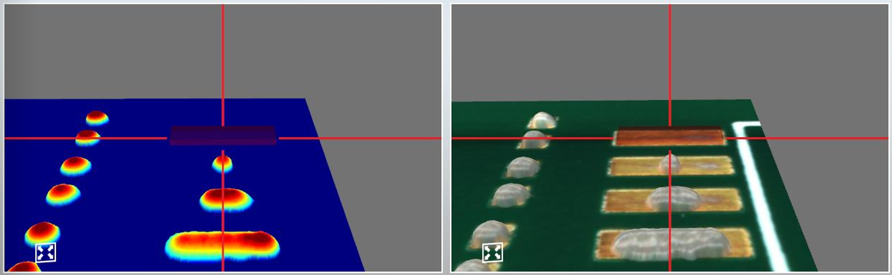
PI series 3D SPI detected deposits with missing solder paste
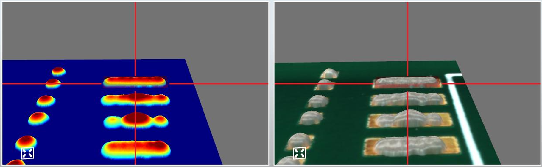
The same deposits after correction with MY700 Jet Printer
Towards a zero-defect future
Whatever the printing method, solder paste type or production environment, these wide-ranging capabilities make jet printing the natural choice for any type of high-quality, high-flexibility manufacturing environment. Fully software-driven and powered by advanced inspection data, the MY700 continues to close even the most challenging quality gaps where the majority of PCB defects tend to emerge: the solder paste printing process.