New advances in machine learning
is raising the bar in inspection technologyIn the SMT industry, we’re seeing how AI and machine learning are being applied to fields like automated optical inspection (AOI) to significantly increase first-pass yield, eliminate potential human errors and boost production.

JUST TEN YEARS AGO, the topic of Artificial Intelligence was an abstract notion in the minds of researchers at MIT, Google and, yes, forward-thinking software experts at Mycronic. Not surprisingly, the idea that machines could think like humans, learn and solve problems, was something of a mindbender. Today, with the advent of machine learning, new machine-to-machine (M2M) protocols like Hermes, Big Data and Industry 4.0, that picture looks very different.
Wanted: more intelligent inspection
“We see huge potential in applying AI to help automate and optimize the entire SMT process — from storage and kitting to line utilization and inspection.” says Olivier Pirou, Head of Product Management and Marketing at Mycronic. “But we’re also trying to pinpoint areas where machine learning can really make a difference right now. To avoid faulty solder joints, defects, false calls and costly rework, for example, we need easier 3D solder paste inspection as well as 3D AOI inspection. It all needs to be interlinked for real-time monitoring, diagnosis and full traceability of images and data. And, of course, the solutions need to be adapted to the new Hermes protocol for M2M communication.”
World-leading inspection expertise
This, in a nutshell, is the focus at Mycronic’s France-based Vi TECHNOLOGY subsidiary. Early pioneers in advanced AOI and SPI inspection, their R&D team now collaborates closely with the Mycronic Group’s AI center in Silicon Valley to bring the power of AI and machine learning to customers. This has led to new AI software platforms and algorithms, unique Z-referencing technology for accuracy and simpler auto-programming tools to eliminate potential human error and free up operators.
New NEO platform for 3D AOI
“Just look at this new board design” says Yan Manissadjian, Product Marketing Manager at Vi TECHNOLOGY, who holds up a high-value board for an aerospace company with thousands of components. “Machine learning reduces the programming time while maintaining the inspection performance,” he says. “And with our new NEO platform for the K series 3D AOI, programming and fine-tuning such a sophisticated board can be twice as fast as with the previous version.”
Available for K Series 3D AOI owners
Mycronic introduced the NEO operating platform at Productronica 2019 in Munich as part of its MYPro Line concept. According to Yan, it’s a key milestone now available as a software upgrade for all K Series 3D AOI customers. The K series 3D AOI system is preferred by demanding producers due to its high reliability, precision and repeatability, regardless of production volumes, he says.
Removing manual steps
“The new inspection system integrates a new generation of algorithms that achieve very high quality, remove manual steps and no longer depend on the skill level of the programmer. By automating programming tasks through autonomous component recognition and assisted model creation, programming time is cut by up to 50 percent,” he says.
Automating the inspection process
The NEO upgrade includes helpful features like Auto MatchMaker and Auto Teach. With the match-making function, all the components available in the library are automatically recognized by the new algorithm when creating the inspection program for a new board. There is no longer any need to do this search manually, one by one: the automatic component recognition takes care of it.
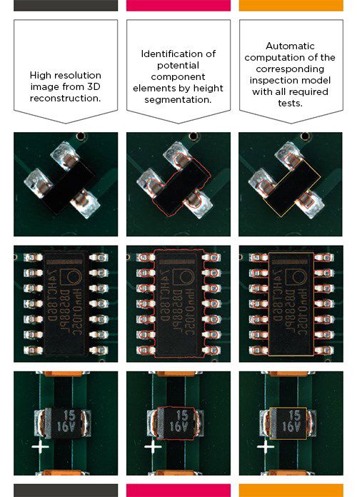
And for adding new components in the central library, the Auto Teach machinelearning algorithm recognizes the shapes of the body and leads, if any, and creates the reference model for inspection by associating the required AOI tests. This new model is then submitted to the operator for approval before being saved in the central library. Creating an inspection model for a new component is now a one-click process.
First pass yield of up to 99 percent
In addition to these great new machine learning features, the NEO platform also includes features to improve the FPY. By scanning each board and instantly adjusting to its actual topography and not to a theoretical or averaged one, operators get an outstanding analytical capability in real time. And with the system’s latest high-speed laser 3D scanning head coupled to a high-precision telecentric optics, the algorithm is fed with extremely accurate raw data and images, resulting in an exceptionally low false call rate. Test coverage has also been extended with the detection of foreign materials, a component overhang test according to IPC requirements, and a new powerful optical verification algorithm. It is this technical rigor and this refusal to compromise that enables our customers to consistently achieve FPY levels of over 95 percent and up to 99 percent in “high reliability” environment.

High-resolution 3D images regardless of component height, material reflectivity, or PCB density.

Handling complex cases: Pin inspection in a deep custom connector from automotive PCB.
Machine learning simplifies 3D SPI
But the company’s 3D AOI inspection systems are not the only area where machine learning is being applied for the benefit of customers. Unique new algorithms are also being embedded into the company’s PI series solder paste inspection system. In a radical twist, this will mean only information that the system cannot detect or reconstruct by itself is requested from the operator — eliminating potential human errors and freeing up operators from certain tasks so they can focus on production.
Measuring the exact height of paste deposits
“The new algorithm allows the system to learn how to locate the paste deposits, without relying only on the location patterns, which are often insuffcient due to the stretch or warpage of the board. It also measures the exact height of a paste deposit taking into account the geometry of the board at this specific location,” says Manissadjian.
Hermes-compatible inspection
“We are also making these systems compatible with the new IPC Hermes digital protocol for better machine-to-machine communication. This started with the PI series 3D SPI machines in Q1 of 2020, and will be followed by our K-Series 3D AOI machines for automated optical inspection in Q4. This is a crucial step in preparing our inspection systems for Industry 4.0,” he concludes.